[Previous] [Contents] [Next]


PC Microprocessor Developments and Features


PC microprocessor design grows more complex with each generation, and CPU packaging keeps changing to provide room for additional features and operating requirements. Microprocessors have evolved from the 4004 described earlier into today's high-speed Pentiums. Each new processor has brought higher performance and spawned new technology. Six basic elements are customarily used to gauge the performance and capability of a CPU design:

  • Speed: The maximum number of clock cycles measured in megahertz. The higher the speed, the quicker a command will be executed.
  • Number of transistors: More switches, more computing power.
  • Registers: The size (in bits) of the internal registers. The larger the registers, the more complicated the commands that can be processed in one step.
  • External data bus: As data bus size increases, so does the amount and complexity of code (information) that can be transferred between all devices in the computer.
  • Address bus: The size of the address bus determines the maximum amount of memory that can be addressed by the CPU.
  • Internal cache: The internal cache is high-speed memory built into the processor. This is a place to store frequently used data instead of sending it to slower devices (speed is relative in computers) such as RAM and hard disk drives. It is built into the processor and has a dramatic effect on speed. We cover cache in more detail later in this lesson.

Intel has held most of the PC CPU market share since the original IBM PC was introduced. Closely following each new Intel launch, rivals such as Advanced Microdevices (AMD) and Cyrix have offered alternative chips that are generally compatible with the Intel models. This development, in turn, drives prices down and spurs a new round of CPU design. Another player is Motorola, a firm that manufactures the microprocessors used in the Apple family of computers, among others.

Intel's 8086 and 8088: The Birth of the PC

We have already introduced the "pre-PC" CPUs. Now we take a look at the models that have powered one of the most dramatic developments of the modern world: the inexpensive, general-purpose computer.

On June 6, 1978, Intel introduced its first 16-bit microprocessor, known as the 8086. It had 29,000 transistors, 16-bit registers, a 16-bit external data bus, and a 20-bit address bus to allow it to access 1 MB of memory. When IBM entered the computer business, the 8086 was too powerful (and expensive) to meet its requirements.

Intel then released the 8088 processor, which was identical to the 8086 except for an 8-bit external data bus, and a slower top clock rate. This meant that 8-bit components (more common at the time) could be used for the construction of PCs, and 8-bit applications written for earlier machines could be converted for PC use. The following table compares the 8088 and 8086 chips.

Chip Number of Transistors CPU Speed (MHz) Register Width External Data Bus Address Bus Internal Cache
Intel 8088 29,000 4.77-8 16-bit 8-bit 20-bit None
Intel 8086 29,000 4.77-10 16-bit 16-bit 20-Bit None

The early 8088 processors ran at 4.77 MHz, while later versions ran at 8 MHz. The 8086 and 8088 processors came as a 40-pin DIP (dual inline package) containing approximately 29,000 transistors. The DIP is so named because of the two rows of pins on either side of the processor, as shown in Figure 4.8. These fit into a set of slots on a raised socket on the motherboard. The small u-shaped notch at one end of a DIP-style CPU denotes the end that has pin 1. During installation, you well need to be sure to line it up correctly, or you might have to repeat the process.

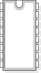
Figure 4.8 DIPP (Dual Inline Package Processor) used for 8086, 8088, and 80286 CPUs

NOTE
The 8088 and 8086 are software-compatible-they can run exactly the same programs (assuming the PCs that use them don't have other complicating factors). The benefit of using an 8086 is its 16-bit external data bus. This allows an 8086-based computer to execute the same software faster than an 8088 computer with the same clock speed.

The early IBM personal computers based on the 8086 and 8088 chips featured:

  • 16 KB of memory.
  • Cassette tape recorder or floppy disk drive for program and data storage.
  • Nongraphics monochrome monitor and monochrome display adapter (MDA).

Soon, a new industry was born as third-party vendors started manufacturing add-ons and improved models of the basic design. Graphics cards with color and better resolution, clocks, additional memory, and peripherals, such as printers, extended the features of the new appliance. "Clones" offered some of these extras at very competitive prices, as a way to attract buyers who wanted a lower price and did not need the comfort of purchasing from a big name like IBM.

NOTE
A clone is a computer that contains the same microprocessor and runs the same programs as a better-known, more prestigious, and often more expensive machine.

Most of the 8088 and 8086-based PCs used some variation of MS-DOS. The variations limited the growth of the software market because of the compatibility issues they presented between versions of MS-DOS. Buyers had to be sure that a program would run on their specific version of MS-DOS.

As users found more ways to take advantage of the PC's power, developers and owners alike soon felt the limitations of the original IBM PC design. The engineers who created it never envisioned the need for more than 16 K of RAM. "Who would ever need more than that?" one is quoted as saying. The cassette drive was never a big seller; most buyers opted for one or two 5.25-inch floppy disk drives, and many soon craved color graphics and the space of the "massive" 5- and 10-MB hard disk drives.

To meet that growing demand, IBM introduced a more robust PC, the XT (eXtended Technology), that could take advantage of a hard disk drive and came with either a monochrome or four-color display and more RAM. Clone makers soon followed suit.

The 80286 and the IBM PC AT

In February, 1982, Intel introduced the 80286 6-MHz microprocessor (later pushing the clock speeds to 10 and 12.5 MHz), commonly called the 286, with a 24-bit address path. In 1983, IBM unveiled its PC AT (Advanced Technology) computer, based on the 286. It had a larger, boxier design, came with a standard hard drive, and a new expansion slot format, rendering older add-on cards obsolete.

The AT could run the same applications as the PC XT (8088), but run them faster. The use of a 24-bit address path allowed the 286 to access up to 16 MB of memory. The clone-makers soon followed suit, taking advantage of third-party versions of the 286. Chip makers Harris and AMD produced versions of the 286 that could run at up to 20 MHz.

Computers based on the 80286 chip featured:

  • Two memory modes (real and protected).
  • 16 MB of addressable memory.
  • Clock speeds up to 20 MHz.
  • Reduced command set (fewer program commands to do more work).
  • Multitasking abilities.
  • Virtual memory support.

Virtual Memory

Virtual memory is the art of using hard disk space to hold data not immediately required by the processor; it is placed in and out of RAM as needed. Although using virtual memory slowed the system down (electronic RAM is much faster than a mechanical hard drive), it allowed the 286 to address up to 1 GB (gigabyte-one thousand megabytes) of memory (16 MB of actual memory and 984 MB of virtual memory). Virtual memory required the use of operating systems more advanced than MS-DOS, leading to the development of products such as Microsoft Windows, IBM OS/2, and SCO's PC version of UNIX.

Real Mode vs. Protected Mode

The 286 might have made older hardware outdated, but Intel had no desire to invoke industry ire and slow the adoption of the new chip by requiring all-new software applications. The result was a CPU with two operating modes: real and protected.

In real mode, sometimes called compatibility mode, a 286 emulates the 8086 processor and addresses only the first 1 MB of memory. This mode is used to run older software. Protected mode allows access to all memory on the system, physical and virtual. In protected mode, a program can write only to the memory allocated to it, with specific memory blocks allocated to different programs. This mode can go well beyond the 16 MB of "true" memory, opening up the possibility of multitasking-running more than one program at a time.

This development required new, more powerful operating systems and applications, but they were slow in coming. By the time they arrived on the market, the 286 was functionally obsolete, but it paved the way for today's powerful multitasking environments such as Windows 95 and 98, Windows NT and 2000. Another major drawback to the 286's memory management scheme was its need to reboot the system when changing between real and protected modes.

The original 286 processor came packaged in DIP (already shown), PGA (pin grid array), and PLCC (plastic leadless chip carrier) designs. The PLCC can be recognized by the arrangement of thin legs around its perimeter. The PLCC's major advantage is its stronger leads (pins), which make it more difficult to damage during removal or installation. PLCCs became popular because they made it easier to upgrade a PC with a faster CPU.

NOTE
PGA and PLCC models look very much alike, but CPUs designed for some types can't be socketed in the other type. Verify the type you need before ordering or attempting a replacement or upgrade (see Figure 4.9).

Figure 4.9 Plastic Leadless Chip Carrier (PLCC) CPU Package

The 80386 Arrives

On June 16, 1985, Intel introduced the original 80386 (commonly known as the 386). This true 32-bit processor was equipped with a 32-bit external data bus, 32-bit registers, and a 32-bit address bus. The first models shipped with a clock speed of 16 MHz, and the CPU sported 275,000 transistors. It could directly address 4 GB of RAM, and 64 TB (terabytes-a terabyte is approximately one trillion bytes) of virtual memory. According to Intel, the 386 could hold an eight-page history of every person on earth in that address space. The 386 was a true generational leap in PC computing, with true multitasking capability-it really could run more than one program at a time. That was due to a third memory mode, called virtual real mode, that allowed independent MS-DOS sessions (called "virtual machines") to coexist on the same system at once. It spawned a host of programs called "memory managers" designed to optimize (and troubleshoot) the more complex world of virtual memory.

The original 80386 chips shipped with speeds of 12 or 16 MHz. Intel produced faster versions-25 and 33 MHz, while AMD manufactured a 40-MHz variant. The 386 provided both the real and protected mode available in the 286.

By April of 1989, the 386 was running at clock speeds of 33 MHz, and Intel was calling it the 80386DX to distinguish it from a lower-cost model, the 386SX.

The 386SX: A Scaled-Down Version

The 386SX came on the scene in June, 1988. Intel wanted to increase the sales of 386-based machines without dramatically dropping the price of its flagship CPU. The result was the introduction of a scaled-down model for "entry-level" computers. It had a 16-bit external data bus and a 24-bit address bus (it could address only 16 MB of memory). The 16-bit configuration allowed it to be used as an upgrade chip for existing 16-bit motherboards, thereby providing an easy transition to the next generation of computers.

The following table compares members of the 80386 chip family from Intel and rival AMD. The AMD 80386DXLV is notable as the first PC CPU with an internal cache.

Chip Number of Transistors CPU Speed (MHz) Register Width External Data Bus Address Bus Internal Cache
Intel 80386SX 275,000 16-25 32-bit 16-bit 24-bit None
Intel 80386DX 275,000 16-33 32-bit 32-bit 32-bit None
AMD 80386DX 275,000 20-40 32-bit 32-bit 32-bit None
AMD 80386DXL 275,000 20-33 32-bit 32-bit 32-bit None
AMD 80386DXLV 275,000 20-33 32-bit 32-bit 32-bit 8 KB
NOTE
The terms "SX" and "DX" are not acronyms; they do not stand for longer terms.

386 Packaging

The 386 was usually placed in either a PLCC package or a PGA package. This type of mount can be found with the 80386, 486, and some older Pentiums up to 166-MHz models. The pins are evenly distributed in concentric rows along the bottom of the chip (see Figure 4.10).

Figure 4.10 PGA (Pin Grid Array)

PGA chips go into regular PGA or the popular ZIF (zero insertion force) sockets. Care must be used when inserting or removing CPUs from a PGA mount-it is very easy to bend the pins if you do not pull perfectly straight up from the socket or have a slight uneven push downward. ZIF mounts are a bit better, but much tech time has been wasted straightening pins, and it is possible to ruin a CPU! PGA mounts are often "hidden" under a CPU fan, which presents another hurdle during repair or upgrade.

A variation of the PGA is the SPGA (staggered pin grid array). It looks almost the same, but with (surprise!) staggered rows of pins. This allows engineers to place more connectors in a smaller area. It also adds emphasis to the caution given earlier about not bending pins through careless removal or insertion.

Both the PGA and SPGA have three pointed corners and a "snipped corner" on one side. Use that corner to line the chip with the socket. If it does not go in smoothly-double check!

Laptop Designs and the Plastic Quad Flat Pack

Some forms of portable PC have existed from the days of the 8088. The early models, such as the Osborne and the original Compaq, were known as "luggables"-tipping the scales at close to 30 pounds. Their cases looked more suited for holding sewing machines than computers. Modern laptop computers started to gain popularity with the advent of the 386 chip and the use of flat screen monitors incorporated in the design, rather than conventional video tubes.

To seat 80286, 80386, and 486 CPUs (the latter are covered in the section that follows) on the more compact laptop motherboards, many vendors use plastic quad flat pack (PQFP) mounts, which are also more secure than traditional socket types designed for systems that will not be moved as much. PQFPs require a submount called a "carrier ring" (see Figure 4.11). PQFPs require a special tool for placing or removing a CPU. Be sure to get the tool before attempting repairs on PQFP-mounted CPUs.

Figure 4.11 PQFP (Plastic Quad Flat Pack)

80486

April 10, 1989, brought us the 80486 line of processors. Once again, the rallying cry was "better and faster." By this time, applications like CorelDRAW, Adobe PhotoShop, and desktop-publishing tools like PageMaker and Ventura Publisher were generating more interest in faster systems. Microsoft Windows was gaining popularity and on its way to becoming the standard desktop environment.

The 486 processor started life at 25 MHz and could address 4 GB of RAM and 64 TB of virtual memory. It is the first PC CPU to break the 1-million transistor mark with 1,200,000. It provided a built-in math coprocessor (older PC CPUs offered separate math coprocessors as an option-usually with a similar number ending in a 7 rather than a 6). The combination speeded up graphics programs that used floating-point math.

The 486SX and Beyond

Once again, Intel sought a way to increase sales without weakening the price of the flagship version of its 486DX CPU, so it added an SX version in April, 1991. This time, the company achieved its goal by removing the math coprocessor, reducing the number of transistors to 1,185,000. Users could upgrade the SX to a 486DX by adding an optional OverDrive processor to restore the missing component.

The 486 label was attached to other chip designs during its active development phase, both by Intel and third-party chip makers. The 486SL, a variant with a 20- to 33-MHz clock and 1.4 million transistors, debuted in 1992. It was very popular in high-performance laptop computers, running at lower voltage (3.3 volts instead of 5 volts) than the usual 486. The small (and for that time) powerful machines also included System Management Mode (SMM), which can dim the LCD screen and power down the hard disk drive-extending the life of the battery.

System Memory Management

System Memory Management (SMM) is a hardware-based function that allows the microprocessor to selectively shut down the monitor, hard drives, and any other peripherals not in use. SMM works at the chip level; the microprocessor can be operating in real, protected, or virtual 8086 mode. SMM is transparent to all software running on the system, which decreases the likelihood of lockups.

Clock-Doubling Debuts

The need for speed spurred the introduction of new models of the 486 family through the spring of 1994, the last variations being the DX2 and DX4. These chips were models with faster clock speeds of up to 100 MHz. The processors were either 25- or 33-MHz versions that had been altered to run internally at double or triple their external speed. For example, the DX4 version of the 486 33-MHz processor ran at 33 MHz externally, but at 100 MHz internally (3 x 33.3 MHz). This meant that internal operations, such as numeric calculations or moving data from one register to another, occurred at 100 MHz, while external operations, like loading data from memory, took place at 33 MHz.

Slower external clock speeds allowed existing motherboard and memory designs to be used. Upgrades were less expensive, and new machines based on the DX technology could quote faster benchmarks at lower costs. The DX4 offered 16 KB of on-board cache, further boosting performance. The DX2 50-MHz-based machines should not be confused with machines designed around the 50-MHz 486DX processor-the latter performed much better.

Vendors such as AMD rode the wave with their own editions of the 486 for users feeling a need for greater speed. The following table lists the most popular 486 chips and third-party work-alikes.

Chip CPU Speed (MHz) Register Width External Data Bus Address Bus Internal Cache
Intel 80486DX 25, 33, 50 32-bit 32-bit 32-bit 8 KB
Intel 80486DX/2 50, 66 32-bit 32-bit 32-bit 8 KB
Intel 80486DX/4 75, 100 32-bit 32-bit 32-bit 16 KB
Intel 80486SX 16, 20, 25 32-bit 32-bit 32-bit 8 KB
Intel 80486SL 16, 20, 25 32-bit 32-bit 32-bit 8 KB
AMD AM486DX 33, 40 32-bit 32-bit 32-bit 8 KB
AMD AM486DXLV 33 32-bit 32-bit 32-bit 8 KB
AMD AM486DX2 50, 80 32-bit 32-bit 32-bit 8 KB
AMD AM486DX4 100, 120 32-bit 32-bit 32-bit 8 KB
AMD AM486DX
"Enhanced"
120, 133 32-bit 32-bit 32-bit 16 KB W/B
AMD AM486DXL2 50, 80 32-bit 32-bit 32-bit 8 KB
AMD AM486SX 33, 40 32-bit 32-bit 32-bit 8 KB
AMD AM486SXLV 33 32-bit 32-bit 32-bit 8 KB
AMD AM486SX2 33 32-bit 32-bit 32-bit 8 KB
CYRX CX486DX 33 32-bit 32-bit 32-bit 8 KB W/B
CYRX CX486DX2 50-80 32-bit 32-bit 32-bit 8 KB W/B
CYRX CX486DLC 33-40 32-bit 32-bit 32-bit 1 KB W/B
CYRX CX486SLC 20-33 32-bit 32-bit 32-bit 1 KB W/B
CYRX CX486SLC2 50 32-bit 32-bit 32-bit 1 KB W/B

Heat Sinks and Fans

The 486 is notable for one other item, the addition of a standard heat sink and, usually, a fan mounted on the CPU and powered by the PC. To maintain stable operation, the PC must provide proper cooling for the 5486 and newer CPUs. Failure of the cooling apparatus can lead to erratic behavior and-uncorrected-can damage the chip. If a customer complains of strange noises inside the PC, the CPU fan is a good place to look. As their bearings age, they start to whine.


[Previous] [Contents] [Next]